

Unpacking 3D Chips: The Future of Silicon Stacking in Semiconductor Technology
Traditional chip scaling hit a wall years ago, leaving engineers scrambling for new ways to boost power without shrinking size. Stacking silicon circuits in layers—what experts call 3D chips—offers a fresh path forward, but making this real took a clever fix using ultra-thin silicon membranes and low-temperature manufacturing. This approach not only improves energy efficiency but also opens doors for AI computing, telecommunications, and other advanced applications. Let’s unpack what this means for the future of semiconductor innovation. Learn more about this breakthrough.
The Challenge Behind Traditional Chip Design
For decades, the semiconductor industry followed Moore’s Law, doubling transistor density approximately every two years. This approach worked well until physical limitations made further miniaturization impractical. As transistors approached atomic scales, issues with heat dissipation, power consumption, and manufacturing costs became significant barriers.
The industry needed a new direction. Rather than continuing to shrink components horizontally, engineers began exploring vertical integration through silicon stacking. This shift represents a fundamental change in how we approach semiconductor design and manufacturing.
Understanding 3D Chips and Silicon Stacking
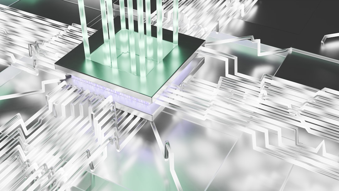
3D chips represent a paradigm shift in semiconductor architecture. Instead of placing all components on a single flat surface, this technology stacks multiple layers of active silicon circuits vertically. Each layer can contain different types of circuits, creating a compact, highly integrated system.
The benefits of this approach include:
Shorter interconnect distances between components
Reduced signal delay and improved processing speed
Lower power consumption due to decreased transmission distances
Greater functional density within the same footprint
Enhanced performance for data-intensive applications
Silicon stacking allows designers to place memory closer to processors, sensors alongside logic circuits, and power management systems within the same vertical structure. This proximity dramatically improves communication between components.
The Breakthrough: Low-Temperature Manufacturing
The major obstacle preventing widespread adoption of 3D chips was the manufacturing process itself. Traditional chip fabrication requires high temperatures that can damage previously built layers when adding new ones on top. This limitation kept true vertical integration out of reach for years.
The solution came through low-temperature manufacturing techniques combined with ultra-thin silicon membranes. By reducing processing temperatures below thresholds that would harm existing circuits, engineers can now safely build multiple functional layers without compromising the integrity of lower levels.
This breakthrough enables:
Sequential layer addition without thermal damage
Preservation of delicate interconnects between layers
Greater flexibility in material selection
Improved yield rates during production
Cost-effective scaling for commercial applications
The use of ultra-thin silicon membranes further enhances this process by reducing thermal mass and allowing better heat dissipation throughout the structure.
Applications Driving Semiconductor Innovation
The practical applications for 3D chips extend across multiple industries. AI computing stands to gain significantly from this technology. Machine learning algorithms require massive parallel processing capabilities and rapid access to large datasets. Silicon stacking brings memory and processing units closer together, reducing latency and improving energy efficiency in AI workloads.
Telecommunications networks, particularly 5G and future 6G systems, demand high-speed signal processing with minimal power draw. 3D chips can integrate radio frequency components, digital processors, and power management in compact modules suitable for base stations and mobile devices.
Other advanced applications include:
High-performance computing clusters for scientific research
Autonomous vehicle processing systems
Medical imaging and diagnostic equipment
Aerospace and defense electronics
Internet of Things sensor networks
Energy Efficiency and Environmental Impact
Energy efficiency represents a critical concern for modern computing systems. Data centers alone consume substantial portions of global electricity, and this demand continues growing. 3D chips address this challenge by reducing the distance signals must travel, directly lowering power requirements.
Shorter interconnects mean less energy lost to resistance and capacitance. When multiplied across billions of operations per second, these savings become substantial. For organizations managing large computing infrastructures, this translates to lower operating costs and reduced environmental footprint.
The Road Ahead for 3D Technology
As low-temperature manufacturing becomes more refined, we can expect broader adoption of silicon stacking across the semiconductor industry. Early implementations will likely focus on high-value applications where performance gains justify development costs. Over time, manufacturing efficiencies will make 3D chips viable for consumer electronics and mainstream computing products.
The semiconductor innovation enabled by this technology extends beyond simple performance improvements. It fundamentally changes how engineers approach system design, allowing new architectures that were previously impossible. This flexibility will drive developments we cannot yet fully anticipate.
Looking Forward
The advancement of 3D chips through silicon stacking and low-temperature manufacturing marks a significant milestone in semiconductor technology. For engineers and researchers working in this space, understanding these developments is essential for staying current with industry trends. The combination of improved energy efficiency, enhanced performance, and new possibilities for advanced applications positions this technology as a cornerstone of future computing systems.
At Britech Group, we recognize that breakthroughs like these create demand for specialized technical talent. Organizations developing or implementing 3D chip technology need professionals who understand both the theoretical foundations and practical applications of silicon stacking. Whether you are an employer seeking experts in semiconductor innovation or a professional looking to work with cutting-edge technology, staying informed about these developments positions you for success in an evolving industry.
Frequently Asked Questions
What makes 3D chips different from traditional semiconductor chips?
3D chips stack multiple layers of active silicon circuits vertically instead of placing all components on a single flat surface. This vertical integration allows shorter distances between components, faster signal transmission, and greater functional density within the same footprint. Traditional chips are limited to horizontal expansion, which has reached practical limits in recent years.
How does low-temperature manufacturing enable 3D chip production?
Low-temperature manufacturing processes operate below thermal thresholds that would damage previously fabricated layers. This allows engineers to build multiple functional layers sequentially without compromising the integrity of circuits already in place. Combined with ultra-thin silicon membranes, this technique makes true vertical integration commercially viable for the first time.
What are the main energy efficiency benefits of silicon stacking?
Silicon stacking reduces the physical distance signals must travel between components, which directly lowers power consumption. Shorter interconnects mean less energy lost to electrical resistance and capacitance. For systems performing billions of operations per second, these small savings per operation add up to substantial reductions in overall power requirements and operating costs.
Which industries will benefit most from 3D chip technology?
AI computing, telecommunications, high-performance computing, autonomous vehicles, and aerospace applications stand to gain the most immediate benefits. These fields require high processing speeds, low latency, and energy efficiency that 3D chips provide. As manufacturing costs decrease, consumer electronics and mainstream computing products will also adopt this technology.
When will 3D chips become available in consumer products?
Early implementations are already appearing in specialized applications where performance gains justify higher costs. As manufacturing processes mature and economies of scale develop, expect to see 3D chips in consumer products within the next 3 to 5 years, starting with premium devices and gradually expanding to mainstream products as production costs decrease.
BriTech Group, Inc.
BriTech Group plays a pivotal role in connecting talented engineers and leaders with growing companies at the forefront of cutting edge technology advancements and other leading innovations. Our expertise helps bridge the gap between demand and supply of skilled technical personnel, fostering a dynamic environment for growth and innovation. To explore more about our spotlights on pioneering technology and innovation, check out this article. For more information about our services, visit BriTech Group.